Thanks to their nanoscale dimensions and large surface-to-volume ratio, the sub-100 nm wide semiconducting nanowires (NWs) undergo a broad range of new physical phenomena, which are non-existing or non-expressed at micrometric scale. Surface charge effects (SCE) are one of these phenomena strongly expressed at nanoscale dimensions and deeply affecting the NW properties, and thus the device performances integrating them, such as piezoelectric (PZ) generators. Despite their crucial influence, SCE are too often neglected in the design of theses NW-based devices, since they are unknown to a large extent and/or non-mastered.
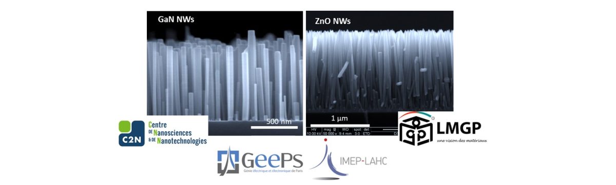
The SCENIC project aims at addressing the fundamental questions regarding the impact of these surface charges in order to control their effects on the properties of sub-100 nm wide GaN and ZnO NWs, two typical NW systems with the same wurtzite structure, in which SCE are highly pronounced. These surface charges being modulated by the material morphology and properties constituting the NWs (nature, dimensions, doping…), and dependent upon the NW functionalization (with inorganic material according to a core-shell configuration, chemical adsorbates…), we propose to investigate different coupling between the active NWs and the environment surrounding them. Based on various nanoscale characterization tools using atomic force microscopy (AFM) in different modes, predictive numerical simulations using finite-element-method including many physical phenomena (i.e. mechanics, electro-mechanical effects, semiconductor physics), and a direct invaluable comparison between the two closed GaN and ZnO NW systems grown by vapor phase techniques (i.e. MBE and MOCVD, respectively) and exhibiting a high crystalline quality, the project will address these crucial nanoscale phenomena in details. By establishing the SCE mechanisms expressed into NWs, the SCENIC project aims at offering SCE nano-engineering solutions for optimizing the surface band bending (surface Fermi level pinning) in link with the targeted PZ application. Then, these advantageous GaN and ZnO NW nano-architectures will be validated through the fabrication and testing of PZ NW-based devices, in which SCE play a major role on their performances.
The SCENIC project is a fundamental project, at a cutting-edge domain of research involving nanomaterials (NWs), physics at nanometer scale (SCE), modelling, and nano- and micro-technology (device validation), with applicative target in the field of piezoelectric generators. The project is based on a complementary partnership between Center for Nanosciences and Nanotechnologies (C2N), Laboratoire des Matériaux et du Génie Physique (LMGP), Group of electrical engineering of Paris (GeePs) and Institut de Microélectronique Electromagnétisme et Photonique and LAboratoire d’Hyperfréquences et de Caractérisation, (IMEP-LaHC). The consortium presents a strong expertise in nanomaterial growth, physical, electrical, chemical characterizations at nanoscale dimensions with specifically advanced and ultimate AFM-based characterization equipments, simulations and device processing and testing, then gathering all the competencies required to address the ambitious objectives of the present project.